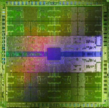
 Graphics technology developer Nvidia has formally introduced its next generation graphics architecture, codenamed Fermi, which Nvidia CEO Jen-Hsun Huang described as putting a supercomputer into a GPU. Unlike traditional GPUs, which are optimized for rendering and graphics tasks, the Fermi architecture is intended to put standard computing operations and graphics procedures on equal footing, enabling developers to leverage the computing power of the GPUs for things like physics simulation, supercomputing, and medical imaging…and, of course, there will still be some applications for gaming.
The Fermi chip currently sports some 3 billion transistors—which compares to 2.3 billion in Intel’s quad-core Itanium and eight-core Nehalem-EX CPUs—and 512 cores, offering eight times the double-precision floating-point performance of previous generations: fast floating point operations are key in many physics simulations. The card can support up to 6 GB of GDDR5 memory, and has six 64-bit memory partitions totaling a 384-bit memory interface. Nvidia is promising developers will be able to tap into the Fermi board using C++ and a Visual Studio development environment dubbed Nexus; the board also offers ECC memory support for catching memory read/write errors.
Nvidia is due to release a beta of Nexus on October 15, although it has not offered any release date or pricing for Fermi products.
Industry watchers generally see Nvidia’s move towards high-performance computing as a good one for the company; although it will face stiff competition from Intel, AMD, and system integrators like HP and Dell, Nvidia’s architecture is sufficiently unique that it could potentially carve out a niche for itself in specialized fiends like climate prediction and image processing and analysis—and margins in the high performance computing market are considerably higher than consumer graphics controllers.


