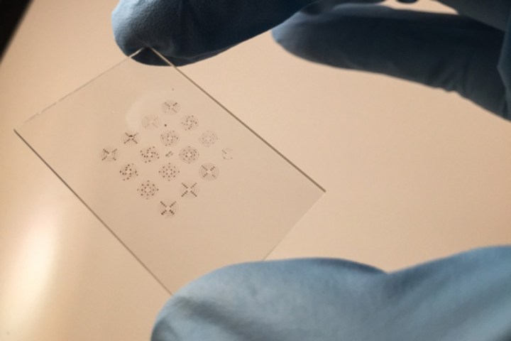
“There is a great need for printing electronics devices,” MIT postdoc and lead researcher Sanha Kim told Digital Trends, “however current methods are mainly limited by the minimum feature size and thickness they can print.”
Kim, Professor John Hart, and their team developed spongy a stamp with nanoscopic pores in order for an ink-like solution of nanoparticles to “stain” and spread uniformly. They grew the stamp out of forests of carbon nanotubes — sheets of cylindrical carbon atoms that Hart had previously engineered into various patterns — which proved to be a prime material.
“Synthesizing carbon nanotubes can make diverse shapes of micro/nano structures with high porosity…and mechanical compliance,” Kim said. “The high porosity provides more space to keep liquid inside the stamp structures and the mechanical compliance provides a good contact which allows uniform transfer of ink during printing.”
The stamp can be printed on firm of flexible surfaces like tape or window panes. Kim also thinks the process may one day let manufacturers print tiny transistors capable of controlling individual pixels.
“The new printing technology will enable printing small thin film transistors and individual [red, green, and blue] pixels for high resolution displays and touch screens, which can be made not only on rigid panels but also flexible, foldable, or stretchable surfaces,” he said. “The new printing technique can also offer relatively cheap, fast way to manufacture large area smart surfaces, like smart mirrors, smart windows, and smart floors.”
A paper detailing the research was published last week in the journal Science Advances.


